تحسين النتائح
ترتيب حسب
من
الى


Matching Properties of Deep Sub-Micron MOS Transistors examines this interesting phenomenon. Microscopic fluctuations cause stochastic parameter fluctuations that affect the accuracy of the MOSFET. For analog circuits this determines the trade-off between speed, power, accuracy and yield.
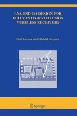
LNA-ESD Co-Design for Fully Integrated CMOS Wireless Receivers fits in the quest for complete CMOS integration of wireless receiver front-ends. With a combined discussion of both RF and ESD performance, it tackles one of the final obstacles on the road to CMOS integration.

This book presents materials fundamentals of novel gate dielectrics that are being introduced into semiconductor manufacturing to ensure the continuous scalling of the CMOS devices. This is a very fast evolving field of research so we choose to focus on the basic understanding of the structure, thermodunamics, and electronic properties of these materials that determine their performance in device applications. Most of these materials are transition metal oxides. Ironically, the d-orbitals responsible for the high dielectric constant cause sever integration difficulties thus intrinsically limiting high-k dielectrics. Though new in the electronics industry many of these materials are wel known in the field of ceramics, and we describe this unique connection. The complexity of the structure-property relations in TM oxides makes the use of the state of the art first-principles calculations necessary. Several chapters give a detailed description of the modern theory of polarization, and heterojunction band discontinuity within the framework of the density functional theory. Experimental methods include oxide melt solution calorimetry and differential scanning calorimetry, Raman scattering and other optical characterization techniques, transmission electron microscopy, and x-ray photoelectron spectroscopy.
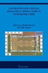
At the system level, a novel systematic study on the full feedforward Sigma-Delta topology is presented in this book. As a design example, a fourth-order single-loop full feedforward Sigma-Delta modulator design in a 130-nm pure digital CMOS technology is presented. This design is the first design using the full feedforward Sigma-Delta topology and reaches the highest conversion speed among all the 1-V Sigma-Delta modulators to date.
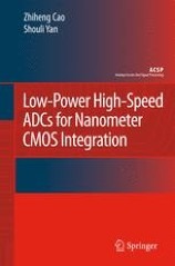
Low-Power High-Speed ADCs for Nanometer CMOS Integration is about the design and implementation of ADC in nanometer CMOS processes that achieve lower power consumption for a given speed and resolution than previous designs, through architectural and circuit innovations that take advantage of unique features of nanometer CMOS processes. A phase lock loop (PLL) clock multiplier has also been designed using new circuit techniques and successfully tested.

Low-Power High-Level Synthesis for Nanoscale CMOS Circuits addresses the need for analysis, characterization, estimation, and optimization of the various forms of power dissipation in the presence of process variations of nano-CMOS technologies. The authors show very large-scale integration (VLSI) researchers and engineers how to minimize the different types of power consumption of digital circuits.
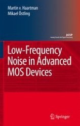
Low-Frequency Noise in Advanced CMOS Devices begins with an introduction to noise, describing the fundamental noise sources and basic circuit analysis. The characterization of low-frequency noise is discussed in detail and useful practical advice is given. The various theoretical and compact low-frequency (1/f) noise models in MOS transistors are treated extensively providing an in-depth understanding of the low-frequency noise mechanisms and the potential sources of the noise in MOS transistors. Advanced CMOS technology including nanometer scaled devices, strained Si, SiGe, SOI, high-k gate dielectrics, multiple gates and metal gates are discussed from a low-frequency noise point of view. Some of the most recent publications and conference presentations are included in order to give the very latest view on the topics. The book ends with an introduction to noise in analog/RF circuits and describes how the low-frequency noise can affect these circuits.
The performance of voltage controlled oscillators (VCO) is of extreme importance for any telecommunication or data communication system. This practical guide develops a systematic, fully-integrated LC-VCO design for low power and low phase noise, especially useful to meet the demands on mobile devices such as cell phones. The proposed VCO design approaches are experimentally verified with several fully integrated CMOS VCOs. The concise presentation is offered in three parts (VCO design; CMOS devices for VCO design; and fully-integrated CMOS DESIGNS) and supplemented by an appendix summarizing the state of the art.
Low Power UWB CMOS Radar Sensors deals with the problem of designing low cost CMOS radar sensors. The radar sensor uses UWB signals in order to obtain a reasonable target separation capability, while maintaining a maximum signal frequency below 2 GHz. This maximum frequency value is well within the reach of current CMOS technologies. The use of UWB signals means that most of the methodologies used in the design of circuits and systems that process narrow band signals, can no longer be applied. Low Power UWB CMOS Radar Sensors provides an analysis between the interaction of UWB signals, the antennas and the processing circuits.

It is essential for circuit and system designers to understand the components of leakage, sensitivity of leakage to different design parameters, and leakage mitigation techniques in nanometer technologies. This book provides an in-depth treatment of these issues for researchers and product designers.
Circuit and Interconnect Design for RF and High Bit-rate Applications covers each of these topics from theory to practice, with sufficient detail to help you produce circuits that are ‘first-time right’. A thorough analysis of the interplay between on-chip circuits and interconnects is presented.

It is shown that in order to achieve high speed and high accuracy at high power efficiency, calibration is required. Calibration reduces the overall power consumption by using the available digital processing capability to relax the demands on critical power hungry analog components. Several calibration techniques are analyzed. The calibration techniques presented in this book are applicable to other analog-to-digital systems, such as those applied in integrated receivers. Further refinements will allow using analog components with less accuracy, which will then be compensated by digital signal processing. The presented methods allow implementing this without introducing a speed or power penalty.

Broadband Opto-Electrical Receivers in Standard CMOS starts from the basic fundamentals, necessary for the design of opto-electronic interface circuits. The book continues with an in-depth analysis of the photodiode, transimpedance amplifier (TIA) and limiting amplifier (LA). To thoroughly understand the light detection mechanisms in silicon, first a one-dimensional and second a two-dimensional model is developed. Analytical design equations are derived to guide the design of the amplifying circuits. For the TIA, the focus lies on the sensitivity-speed trade-off. For the LA, a high gain-bandwidth is pursued. Several practical design examples reveal the subtleties and challenges encountered during the design of high-performance analog circuits.
"Analog-Baseband Architectures and Circuits reviews the fundamentals and studies the state-of-the-art multistandard transceivers before describing novel architectural and circuit techniques for implementing multimode and wideband (tens of MHz) baseband analog front-ends under low-voltage constraints. Techniques developed on architecture level for efficient system-in-package (SiP) integration, testability and multi-standardability; and on circuit level for reducing the required supply voltage, power and area are generally applicable for most wireless systems, and are somewhat independent to technology scaling. Experimental 1-V baseband building blocks (i.e., double-quadrature-downconversion filter, programmable-gain amplifier and dc-offset canceler) and a 1-V fully-integrated receiver analog-baseband chain for IEEE 802.11a/b/g WLAN validate the techniques. The implementations are all in standard-VTH CMOS process, and no voltage boosting is required at any node." "Analog-Baseband Architectures and Circuits will be relevant to system architects, circuit designers, professors and students engaged in wireless transceiver front-ends research and development."
The book starts with elementary stages in building up operational amplifiers. The synthesis of opamps is covered in great detail, such that lowest power consumption is always guaranteed. Many examples are included, operating at low supply voltages. Chapters on noise, distortion, filters, ADC/DACs and oscillators follow. These are all based on the extensive amount of teaching that the author has carried out both at universities and companies world-wide. All chapters have been drawn up specifically for self-study. They aim, however, at different levels of understanding. All start with elementary material. Most chapters also contain advanced material, especially from Chapter 9 onwards.
This book is part of the Analog Circuit Design series and contains the revised contributions of all speakers of the 16th AACD Workshop, which was organized by Jan Sevenhans of AMI Semiconductor and held in Oostende, Belgium on March 27-29, 2007. The book comprises 17 tutorial papers, divided in three chapters, each discussing a very relevant topic in present days analog design.
This book is number 15 in this successful series of Analog Circuit Design, providing valuable information and excellent overviews of analog circuit design and related CAD, mainly in the fields of basic analog modules, mixed-signal electronics, AD and DA converters, RF systems, and automotive electronics.
The book is a comprehensive elaboration on important topics which capture major research and development efforts today. The motivation and inspiration behind this book is to deliver a thorough text that focuses on the evolution of test technology, provides insight about the abiding importance of discussed topics, records today’s state of the art and industrial practices and trends, reveals the challenges for emerging testing methodologies, and envisages the future of this journey. The book consists of eleven edited chapters written by experts in Defect-Oriented Testing, Nanometer Technologies Failures and Testing, Silicon Debug, Delay Testing, High-Speed Test Interfaces, DFT-Oriented Low-Cost Testers, Embedded Cores and System-on-Chip Testing, Memory Testing, Mixed-Signal Testing, RF Testing and Loaded Board Testing.

Microsystems in many cases provided the key functions for this progress. Although the issues the event concentrated on didn’t change significantly (safety, powertrain, comfort, etc.), considerable shifts of technological paradigms and approaches can be stated. The future of microsystems will consist of integrated smart systems which are able to diagnose a situation, to describe and to qualify it. They will be able to identify and mutually address each other. They will be predictive and therefore they will be able to decide and help to decide. Smart systems will enable the automobile to interact with the environment, they will perform multiple tasks and assist a variety of activities. Smart systems will be highly reliable, often networked and energy autonomous.
Provides a comprehensive monograph on gate stacks in semiconductor technology. The reader will get a clear view of what has been done so far, what is the state-of-the-art and which are the main challenges ahead before we come any closer to a viable Ge and III-V MOS technology.

سوريا - اتستراد درعا - غباغب
+963-15 2050 - 15 860 380 /1/2/3 - 11 662 3900